Single Atom Thick Tin Sulfide : Big Potential from Simple Ingredients
Imagine a material so thin it’s only a single atom thick – yet it could turbocharge tomorrow’s electronics. Scientists have now done just that with tin sulfide (SnS), creating ultra-thin sheets of this semiconductor using nothing more than plain tin and sulfur. This single atom thick crystal isn’t just a lab novelty; it conducts electricity and interacts with light in unique ways. “SnS is special because it can conduct electricity and respond to light in unique ways,” explains researcher Makoto Kohda. By making SnS so thin and pure, researchers believe they can harness those unusual properties to build faster, more efficient devices.
Just Tin and Sulfur: A Simple Recipe for Monolayer SnS
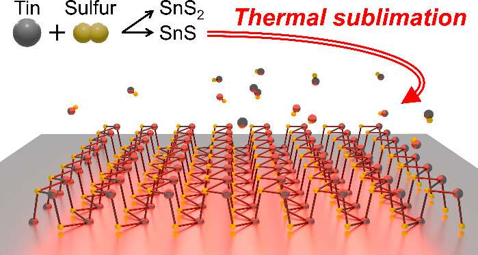
Producing SnS as a monolayer used to be a challenge. If the conditions weren’t perfect, you might grow the wrong material (SnS₂ instead of SnS) – like a waiter accidentally bringing the wrong dish. The breakthrough from Tohoku University and collaborators is a brilliantly simple recipe: just heat tin and sulfur together in the right way, and you can grow pure, high-quality SnS crystals on an ordinary silicon wafer.
A computer-calculated phase diagram predicted that keeping the sulfur vapor level low would yield SnS, while too much sulfur would yield SnS₂. So the team literally adjusted the distance of the sulfur source (imagine moving a spice jar closer or farther) to control how “seasoned” the reaction was with sulfur. This ensured the crystal that formed was exactly the desired SnS every time, not its look-alike cousin.
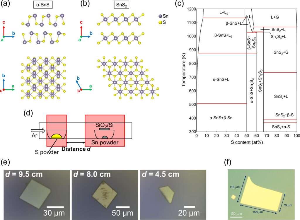
By carefully heating tin (gray) and sulfur (yellow) on a silicon wafer, researchers grew a sheet of tin sulfide only one atom thick. By adjusting the amount of sulfur vapor – like tweaking an ingredient in a recipe – they made sure to get SnS (tin monosulfide) instead of accidentally making SnS₂. In the experiment, they even watched through a microscope as extra layers of the crystal “sublimed” away (turned directly from solid to gas) at high temperature, leaving behind a single atom thin film. The result of this process is large, ultra-thin SnS sheets that are easier to obtain than ever.
Some of these 2D SnS crystals reached tens of micrometers across – roughly the size of a fine grain of sand or about half the width of a human hair. That may sound tiny, but in the world of atom-thick materials it’s huge, large enough to start imagining real devices built from them. Importantly, the method uses only basic elements as sources, avoiding toxic or costly chemicals. This safe, cost-effective strategy is expected to streamline the production of SnS, meaning researchers everywhere can more easily explore its potential.
In fact, the team watched their SnS sheets form in real time and noted that having high-quality monolayers at hand “could speed up how scientists discover and understand new physical effects using monolayer SnS”. In other words, this simple growth technique is opening the door for rapid innovation using SnS.
Unique Properties at Single Atom Thick
Why are scientists so excited about a sheet of tin sulfide only a few atoms wide? It turns out that monolayer SnS has a rare combination of traits that could make it a technological threat.
SnS is ferroelectric even at a single atom thick. In a ferroelectric material, tiny positive and negative charges naturally line up within the crystal, creating a built-in electric polarization. Uniquely, SnS holds this polarization in-plane (along the sheet) and can switch its direction when an external field is applied. This is remarkable at the monolayer level – it’s like a nanoscale memory that remembers an “ON” or “OFF” electric state without needing power. Engineers dream of using such ferroelectric behavior for new memory devices or even for novel optical gadgets. For instance, one proposal is to use a monolayer SnS as an ultrathin light filter (polarizer) that can be electrically switched on and off by flipping its polarization.
SnS’s low crystal symmetry also gives rise to unusual optical and electronic effects. Because the atoms in monolayer SnS are arranged without an inversion center (there’s no perfect mirror symmetry through the layer), shining light on it can directly generate an electric current – a phenomenon known as the shift-current photovoltaic effect.
In simpler terms, SnS can act a bit like a solar cell or photodetector even in its pure form: when light hits it, electrons prefer to flow one way, producing a current without any external voltage. This built-in light response could be harnessed to make ultrathin photodetectors or energy-harvesting devices that operate on the nanoscale. And since SnS is just single atom thick, such a photodetector would be extremely compact and could even be transparent.
Perhaps the most futuristic aspect of SnS lies in the spin of its electrons. Each electron has a property called spin – you can imagine it as a tiny compass needle that can point “up” or “down” – and this spin can carry information. Monolayer SnS interacts with electron spins in a special way due to its heavy tin atoms and asymmetric structure. The material is predicted to support a phenomenon charmingly called a persistent spin helix, which is essentially a very stable wave-like arrangement of electron spins.
Normally, spin patterns in a material randomize quickly, but in SnS the spins can stay coordinated over a long distance. This means data encoded in the spins (for example, “spin up” as 1 and “spin down” as 0) could travel without getting scrambled. Researchers say this persistent spin alignment is expected to enable spin-based logic devices, where the usual electrical current in circuits could be replaced by currents of aligned electron spins. In essence, SnS could act as a highway for spinning electrons, allowing for spintronic computing elements that might switch faster and waste less energy than traditional transistors.
From Light Sensors to Spintronics: What’s Next?
All these exotic-sounding properties aren’t just for show – they hint at real next-generation gadgets. Because a monolayer SnS can combine electrical, optical, and spin-based functionalities, it’s like a Swiss army knife of future electronics. For example, an atom-thin SnS film could work as a super-sensitive photodetector, converting incoming light directly into an electrical signal for an ultracompact camera sensor or optical communication chip. Its built-in ferroelectric polarization means it could serve as a tiny non-volatile memory bit or an electrically tunable filter for light.
At the same time, the stable spin configurations in SnS open the door to spin logic circuits – essentially, transistors that use the orientation of electron spins to represent 0s and 1s instead of electric charge. Such spin-based devices could operate with much lower power and higher speeds, since flipping a spin takes less energy than moving a bunch of electrons around. By controlling both spin and valley, future spin–valleytronic devices could perform operations in new, parallel ways that standard electronics can’t match.
The excitement surrounding SnS comes from the convergence of these abilities in one tiny material. Researchers point out that this single atomic layer ties together three hot research fields at once – ferroelectrics, spintronics, and valleytronics – which could “open the door to creating better electronics,” especially those that use light and tiny spins to work faster and smarter. And now that large, high-quality monolayer SnS can be made with a simple and scalable method, its journey from the lab to practical use looks more feasible.
We might soon see prototypes of new photodetectors, memory devices, or even computing architectures that exploit SnS’s unique trifecta of properties. In a sense, turning basic tin and sulfur into an ultra-thin, powerful semiconductor almost feels like modern alchemy – a simple mixture yielding a futuristic material. It’s a vivid reminder that sometimes the next big thing in technology can come from just a couple of the simplest ingredients, cooked up in the right way.
Content
Selective Synthesis of Large-Area Monolayer Tin Sulfide from Simple Substances
Kazuki Koyama, Jun Ishihara, Nozomi Matsui, Atsuhiko Mori, Sicheng Li, Jinfeng Yang, Shiro Entani, Takeshi Odagawa, Makito Aoyama, Chaoliang Zhang, Ye Fan, Ibuki Kitakami, Sota Yamamoto, Toshihiro Omori, Yasuo Cho, Stephan Hofmann, and Makoto Kohda
Nano Letters 2025 25 (25), 9985-9993
DOI: 10.1021/acs.nanolett.5c01639
Source: https://thebulklab.com